Silicontrivance
Description
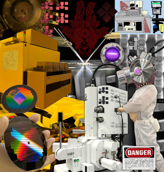
This piece is a collage tribute to nanofabrication and the UCSB Nanofab, a cleanroom facility used by researchers to make microelectronic devices. Over the past half year, I have been an intern in the Nanofab, and been fortunate enough to use and care for many of the wonderful machines within.
This piece is a collage of photos and illustrations related to the UCSB Nanofab. I wanted to make the collage whimsical, eclectic, and overwhelming in a comforting way, much like the fab itself. Pictured is a JEOL scanning electron microscope (SEM, center), an ASML PAS5500 lithography stepper (left), a dancing figure in a bunnysuit with an illustrated head resembling metal vacuum chambers with plasma, a devious drawn figure inspired by optical waveguides (top center), an MS Paint drawing of a plasma etching tool (top right), wafers I made using the stepper (bottom left), nMOS transistors my labgroup and I made in the Teaching Cleanroom, micrographs I took on the SEM, electrical probe tips (center), and the eye of my favorite machine–the objective lens of the ASML stepper (top left).