Net of Nuclei
Description
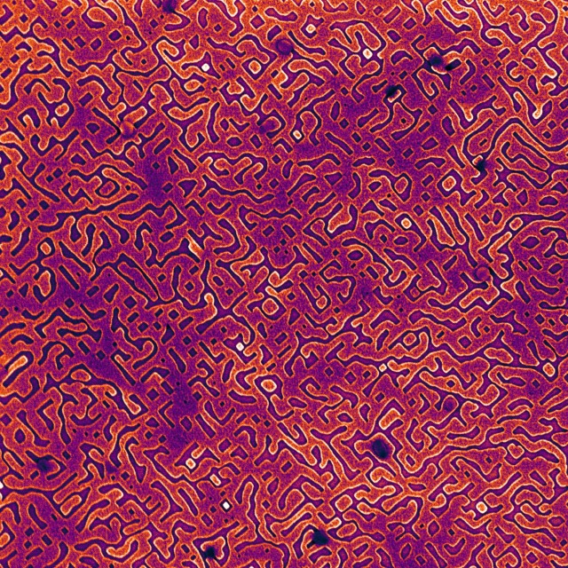
When growing thin films of crystals, we want the film to spread out and cover the entire substrate in a smooth layer, but then this image would be blank… In reality this coating can be inconsistent – here we see PbSe beading up like water on glass to form a complex web of droplets on a GaAs surface.
These lines of PbSe you see here are only about 20 nanometers wide - that's painting with a pretty fine brush! This image was taken with the FEI Nova Nano scanning electron microscope in SE (Secondary Electron) mode. This imaging condition is sensitive to surface topography, so the lines you see are literally little flat mesas of PbSe that crisscross the surface of a GaAs substrate. From a research perspective, the most important feature of this image is the ordering of the islands – if you look carefully, all the edges seem to line up – the way this image is cropped, they point toward the diagonals. This pattern originates in the deeper crystallographic symmetry of PbSe – it has the same structure as common table salt, and left to its own devices, it would much rather make cubes!


