Morphology of a semiconducting polymer
Description
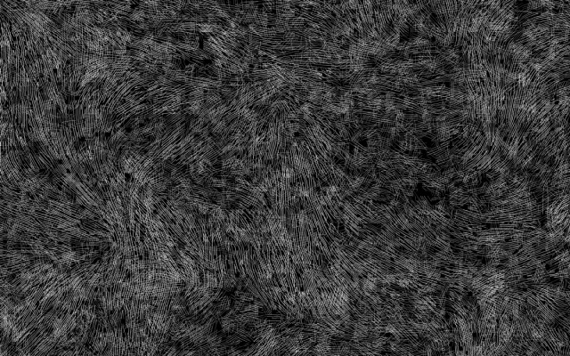
Semiconducting polymers have great potential for a wide variety of low-cost, flexible electronics. The electrical properties are determined, in large part, from their arrangement in the thin film across many length-scales. Based on the analysis of a high-resolution electron micrograph, solid lines have been drawn parallel to the average direction of the polymer backbones. Looking through the film one observes long, flowing, and overlapping/woven structures that illustrate the complexity and elegance of the self-assembly at the nano- and micron-scale. The polymer backbones often locally align over several hundreds of nanometers and form domains. The overlapping/woven regions bridge the domains together, forming a highly interconnected morphology that is believed to benefit the electronic properties.
Commercial polymer name: Polyera P(NDI2OD-T2).
The image is 1500 nm x 940 nm.