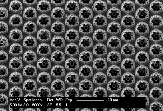
Gallium Nitride Flowers
Year:
2015Ranking:
EntrantArtist:
Sang Ho Oh (Graduate Student)Lab:
DenBaars LabDescription
This is an SEM image of roughened backside of the LED device that was grown on a freestanding GaN substrate, which is to extract more light from the LED device. Small dot (a few microns) patterns are transferred to the backside of the LED device through the photolithography, and than the surface is roughened by ICP (inductively coupled plasma) dry etch. The etch should result in the set of perfect cones. However, in this case, somehow the cones were not formed, but the flower-like shapes were produced.